Plastic material solutions for semiconductor industry
Plastic material solutions for the semicond industry
Of all the industries in which engineering plastics can help engineers solve design problems, no industry is more challenging than the semiconductor industry. Our plastics used in the semiconductor industry have always been designed with the harsh environmental problems of the industry in mind. In addition, our semiconductor industry experts also work directly with engineers to understand the unique challenges in all aspects of the semiconductor manufacturing process, from pre wafer processing to chip processing and processing and even post packaging.
Each stage of processing faces difficulties, including extremely high temperature, exposure to highly aggressive chemicals, contact with abrasive solvents and vacuum plasma, etc. Ensinger has plastic solutions suitable for various environments, meeting the most stringent requirements of design, processing tolerances, gas leakage and pollution specifications. Our design solutions cost less than traditional materials such as ceramics or quartz and are generally easier to use.
Processable plastics for semiconductor industry
Ceramic peek
An advanced proprietary nano ceramic filled PEEK composite is created to meet the strict tolerance requirements of high-frequency integrated circuit chip socket test fixture.
TORLON 4203 natural
Excellent compressive strength, elongation, electrical insulation and excellent impact strength - are commonly used in IC test seats, processing, as well as electrical connectors and insulators.
ESD plastics
Our ESD (electrostatic dissipation) materials have a surface resistivity of 106 to 109 watts / m2. They are usually used in clean rooms to reduce static electricity and are widely used in the field of semiconductors. Fixture for manufacturing silicon wafer and equipment in semiconductor equipment.
PEEK natural
PEEK is a kind of plastic with high thermal performance and no permanent loss of steam to PEK. In harsh environment, it is a high strength alternative to fluoropolymers. Peek has a combustion grade of V-0 and has very low emissions of smoke and toxic gases.
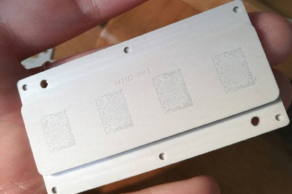
Test socket
In the process of microchip manufacturing, it is important to test the chip under various conditions to ensure its specific function and durability. Different test sockets are used to test various microchips designated by IC designers. As various engineering plastics are used to make different test sockets, the demand for plastic materials continues to grow rapidly.
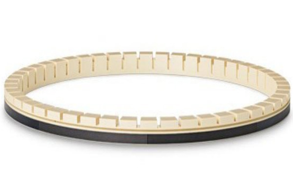
Grinding ring
Chemical mechanical polishing (CMP) process is a very important step in silicon wafer production. The larger the wafer size, the smaller the chip, and the smaller the line width and grain size on the chip. Finding the ideal material to meet the performance requirements is a big challenge, because the CMP process requires components made of high-performance materials. Through close cooperation with customers, we continue to develop and promote the brand to develop this material in combination with practical applications.